

Why the Package Is the New Moore’s Law in AI Chips
Authored by Jaskaran Singh Dhiman
A few months ago, someone asked me a simple question: What is the smallest transistor on a chip? I opened my mouth to answer, saying 2 or 3 nm nodes, but realized I did not know. This made me think that it probably did not matter, as no one had shrunk the transistor at the same pace in the last decade as compared to the last 4-5 decades. Moore’s law has not been able to keep up, which has pushed the semiconductor industry to innovate the package style instead of reducing the node size.
That small, slightly embarrassing moment is the whole story of where chip performance comes from now, so let us talk about it: why the transistor stopped being the headline, what quietly took its place, and what it looks like from the advanced packaging perspective.
The following is a method for visualizing this. For decades, building a faster chip was like building a taller building — adding floors, getting more space, and repeating. This is Moore’s Law: shrink the transistor, fit more on the same sliver of silicon, and performance follows almost automatically. However, every city eventually reaches a point where height alone stops solving the problem. You cannot fit more people into a taller tower if the elevators, hallways, and utilities connecting the floors cannot keep up with the increased demand for space. At some point, the real bottleneck stops being how tall you can build and starts being how well everything inside is connected.
The problem in numbers
Transistor density used to double roughly every two years, and now that cadence has stretched closer to three years. Each step forward also costs dramatically more for a smaller gain: design cost estimates put a 28 nm node chip at roughly $51 million, 7 nm at about $298 million, and 5 nm at approximately $542 million, with 3nm running from $500 million to $1.5 billion depending on complexity [1]. “Smaller node, faster chip” no longer explains the real gains, because the constraint has shifted to how fast memory and logic communicate with each other rather than the individual component performance.
Why it’s easy to miss
This shift does not make headlines the way new node names break into production. However, the advanced chip packaging market is projected to roughly double, from approximately $44 billion in 2025 to $88 billion by 2030, outpacing the semiconductor industry overall [2]. Anyone still asking “what node is this chip built on” is asking a wrong question and is slightly out of date. The actual question should be how the package performs in terms of power delivery, data movement, and heat dissipation.
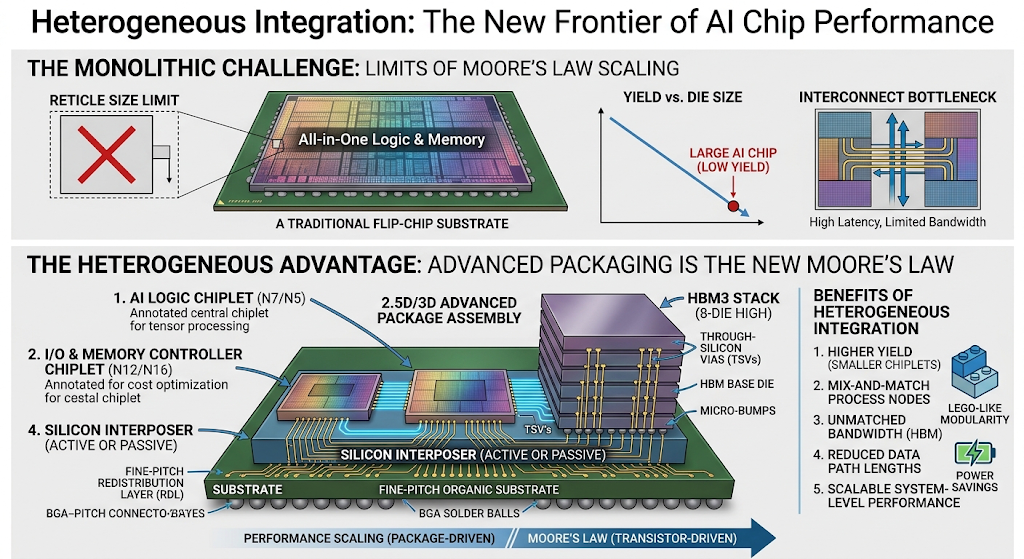
Image Source: Generated by AI
What is scaling
If the transistor is not the number to watch, then the question is what to keep an eye on. Older packages connected dies with solder bumps spaced approximately 50 to 130 microns apart. Hybrid bonding technology has already pushed this below 10 microns, with roadmaps targeting 3 to 4 microns [3], roughly a thousandfold jump in connection density. Memory is scaling just as fast: HBM3 delivers approximately 819 GB/s per stack, HBM3E over 1.2 TB/s, and HBM4 targets over 2 TB/s by doubling its interface width [4], with stack heights increasing from 8 layers to 16. None of that comes from a smaller transistor; it comes from how densely and reliably the pieces are packaged together. Part of that is advanced packaging technology, Thermal Compression Bonding (TCB) equipment that I work on.
What it looks like from the equipment side
I work on the equipment that connects the die with heat and pressure, precisely enough that hundreds of microscopic connections line up at once. Two aspects of that work show what this shift demands in practice.
- The margin for error decreases more rapidly than the pitch itself. At ultra-low pitch interconnection, there is no room for a cleanup step after the fact. Any residue on the copper pad becomes a permanent defect, which requires cleaning the surface immediately before bonding within a time window of seconds.
- A breakthrough is significant only if it can be implemented on a large scale. A bonding process that works beautifully on a handful of wafers per day does not help an industry at the pace of shipping well over 2 million AI servers per year [5]. Changing the machine architecture from a single to a dual head helps run two processes in parallel instead of sequentially, which theoretically delivers a roughly 2x increase in throughput without any new bonding chemistry.
Neither of these is a transistor problem. Both are the exact problems that determine how fast AI hardware reaches the market.
Therefore, if someone asks me that question again — what the smallest transistor in this chip is — I have a better answer now: probably not much smaller than the last one. Instead, ask how tight the pitch is, how many gigabytes per second are moving between memory and logic, and how many of those connections a machine can make correctly every single time. That is where the real story and the new talk of the trend lie.
Jaskaran Singh Dhiman is a Staff Engineer in Operations Engineering – NPI, Advanced Packaging at Kulicke & Soffa Industries, where he leads the production readiness of thermocompression bonding systems used in advanced packing.
References
[1] Semiconductor Engineering, “Big Trouble At 3 nm,” Nov. 2024. [Online]. Available: https://semiengineering.com/big-trouble-at-3nm/
[2] BCC Research, “Advanced Chip Packaging Technologies Market to Reach $87.6 Billion by 2030, Driven by AI and High-Performance Computing Demand,” GlobeNewswire, Aug. 11, 2026. [Online]. Available: https://www.globenewswire.com/news-release/2026/08/11/3342689/0/en/advanced-chip-packaging-technologies-market-to-reach-87-6-billion-by-2030-driven-by-ai-and-high-performance-computing-demand.html
[3] Basler AG, “Hybrid Bonding: The New Precision Bottleneck in Advanced Packaging,” Feb. 2026. [Online]. Available: https://www.baslerweb.com/en/learning/semicon-hybrid-bonding/
[4] Rambus, “High Bandwidth Memory (HBM): Everything You Need to Know,” Mar. 2026. [Online]. Available: https://www.rambus.com/blogs/hbm3-everything-you-need-to-know/
[5] TrendForce data, cited in “Comparing HBM, HBM2, HBM3 and HBM3e,” Aivon, Feb. 2026. [Online]. Available: https://www.aivon.com/blog/memory-storage-technology/comparing-hbm-hbm2-hbm3-and-hbm3e/